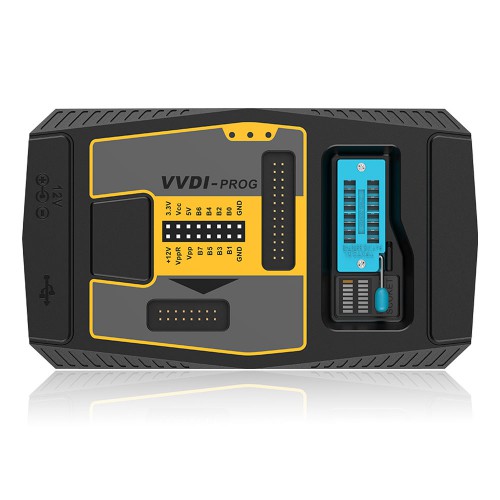
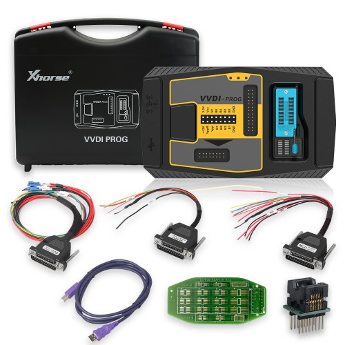
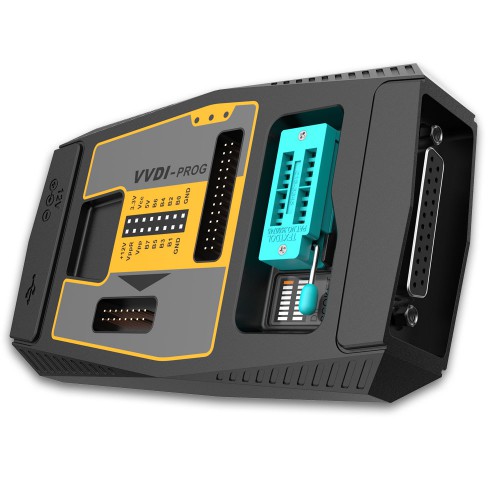
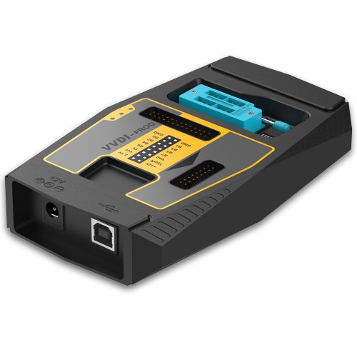
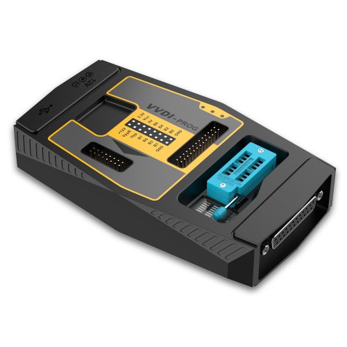
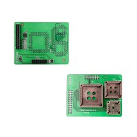
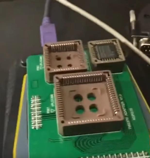
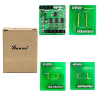
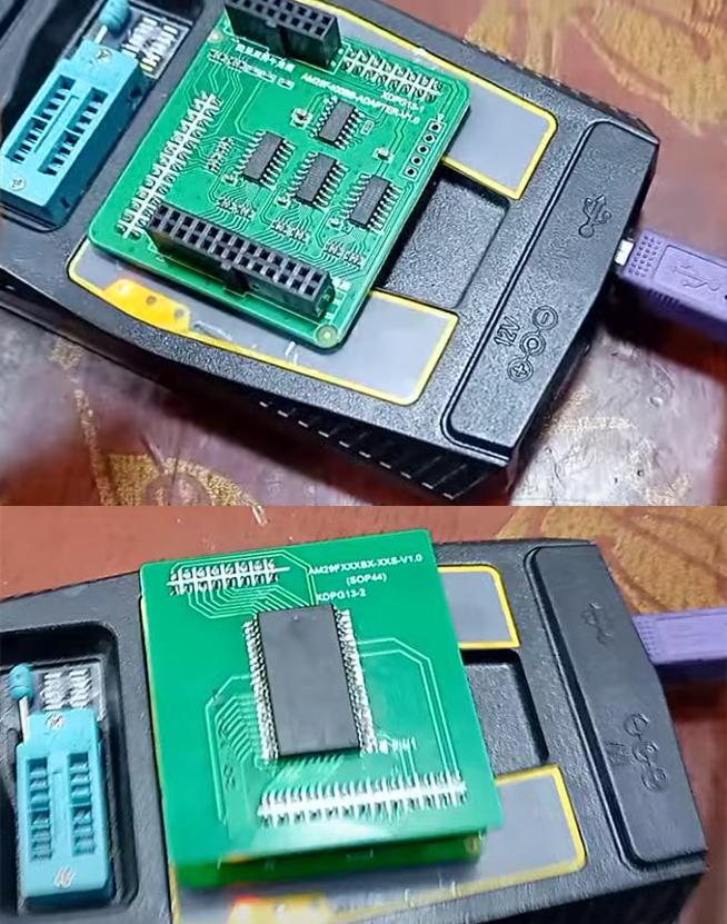
Xhorse V5.3.5 VVDI Prog Programmer with Full 11 Adapters Newly add BOSH ECU Adapter DHL Free
EU Ship, NO Tax!
All 4% OFF, except bottom price items.
Better price, please contact Susie!
Skype: xhorsevvdi.com
Whatsapp:+86-13983756354
Product Description
Note:
From now on, package not includes SO370 Xhorse TB28FXX Adapter.
TOP 5 Reasons to Get Xhorse VVDI PROG:
1. VVDI PROG Software: V5.3.5
VVDI PROG Firmware: 2.0.0
2. Multi-Language: English, Arabic, Czech, French, Italian, Polish, Portuguese, Russian, Spanish, Turkish, Chinese
3. VVDI Prog read BMW ISN
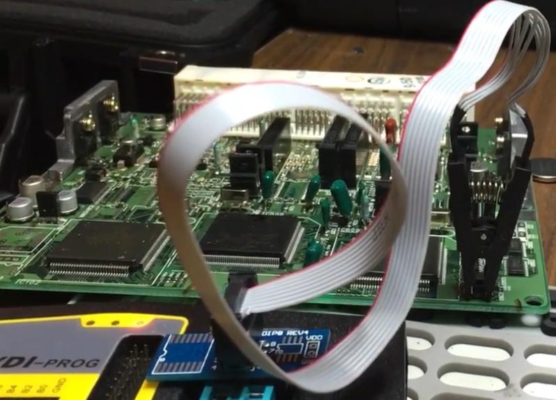
Once you buy VVDI Prog programmer, you can get free BMW ISN read function and NEC, MPC, Infineon etc chip continuously update service. If it supports to read BMW ISN, after click read, it will show the ISN automatically like follow pic shows.
4. Xhorse VVDI PROG Support UK/Russia Local Shipping, NO Tax, Arrive Fast.
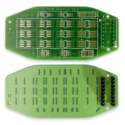
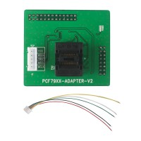
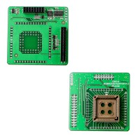
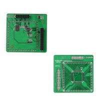
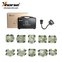
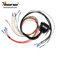
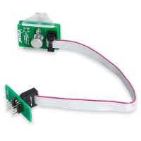
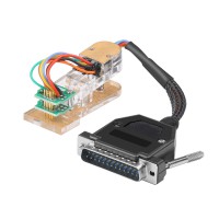
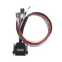
5. The package includes VVDI PROG Default package and 11 optional adapters.

VVDI Prog and Optional Adapters List:
|
Adapter Name |
Price (USD) |
Adapter Image |
Function |
Wiring Diagrams/Pages |
|
44.99 |
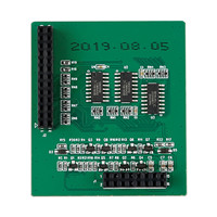 |
Read/Write AB28FXXX/PA28FXXX/TB28FXXX |
null |
|
|
39.99 |
|
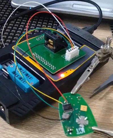
Read/Write PCF7922 PCF7941 PCF7945 |
 |
|
|
39.99 |
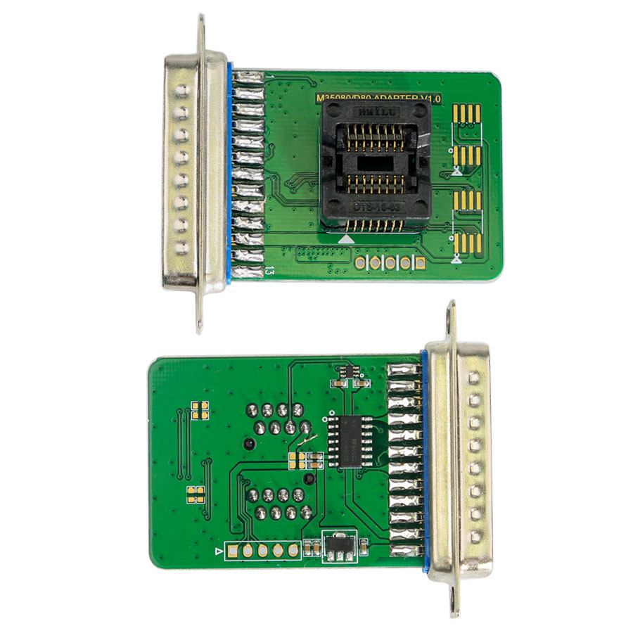 |
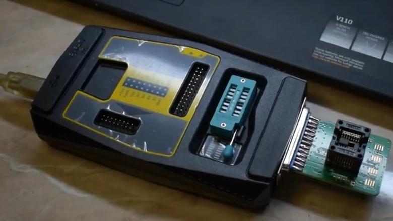
Read/Write M35080, M350803, M350806, |
 |
|
|
39.99 |
|
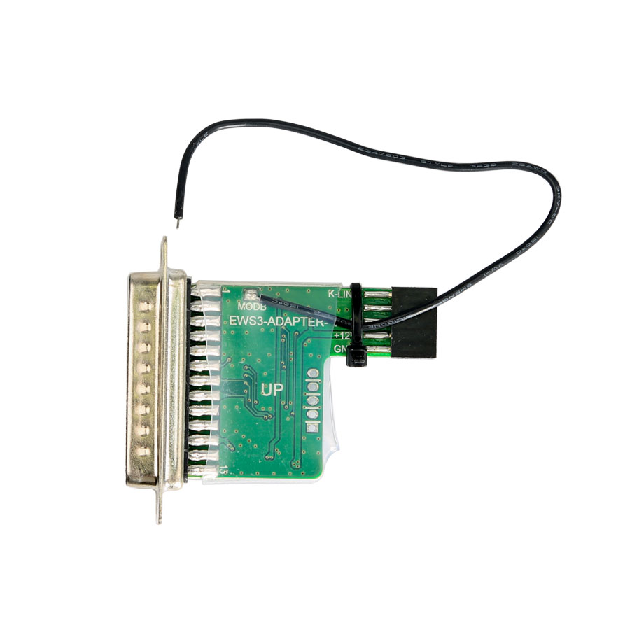
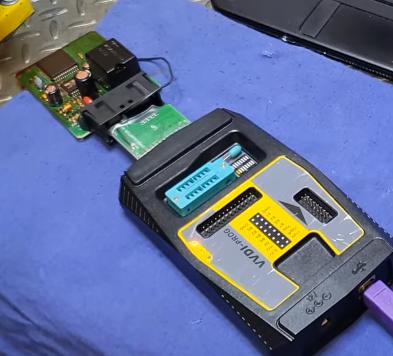
Read BMW EWS3 data without soldering |
 |
|
|
39.99 |
|
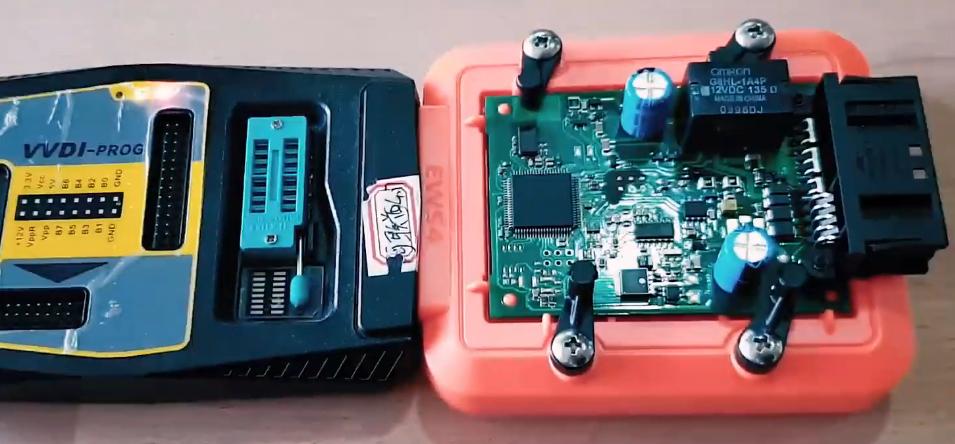
Read BMW EWS4 data without soldering |
 |
|
|
50.00 |
|
Read/Write |
|
|
|
29.99 |
|
Read/Write TMS370 (PLCC28 package) chip |
|
|
|
39.99 |
|
Read/Write AM29FXXXB series chip |
|
|
|
29.99 |
|
Read/Write MC68HC05BX (PLCC52 package) chip including 0D60J, 1K20C, 3G96A (old Epia BCM) |
null |
|
|
29.99 |
|
Read/Write MC68HC05X32 ( QFP64 package) chip including OD69J, 1D69J, 1H52A, 0G47V (MC68HC05 series Mercedes EIS / EZS) |
null |
|
| 69.00 | 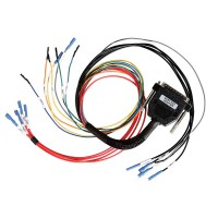 |
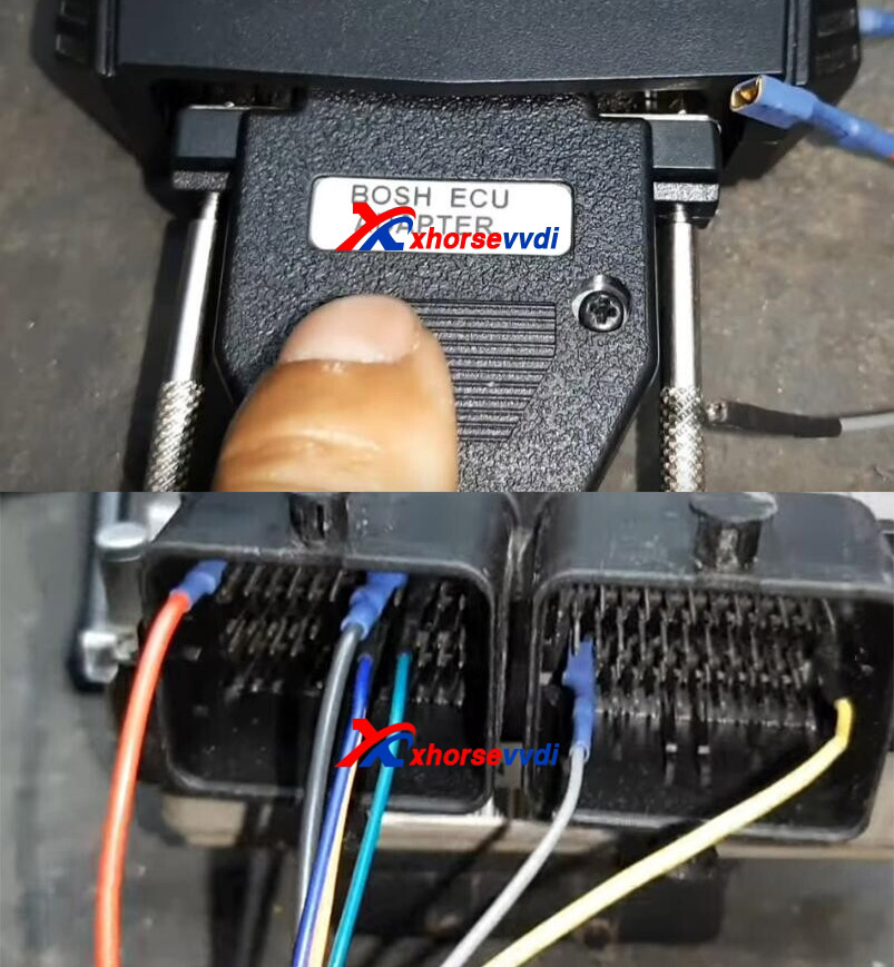
Read BMW ECU N20 N55 B38 ISN Without Opening |
 |
|
| 269.00 | 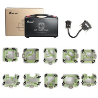 |
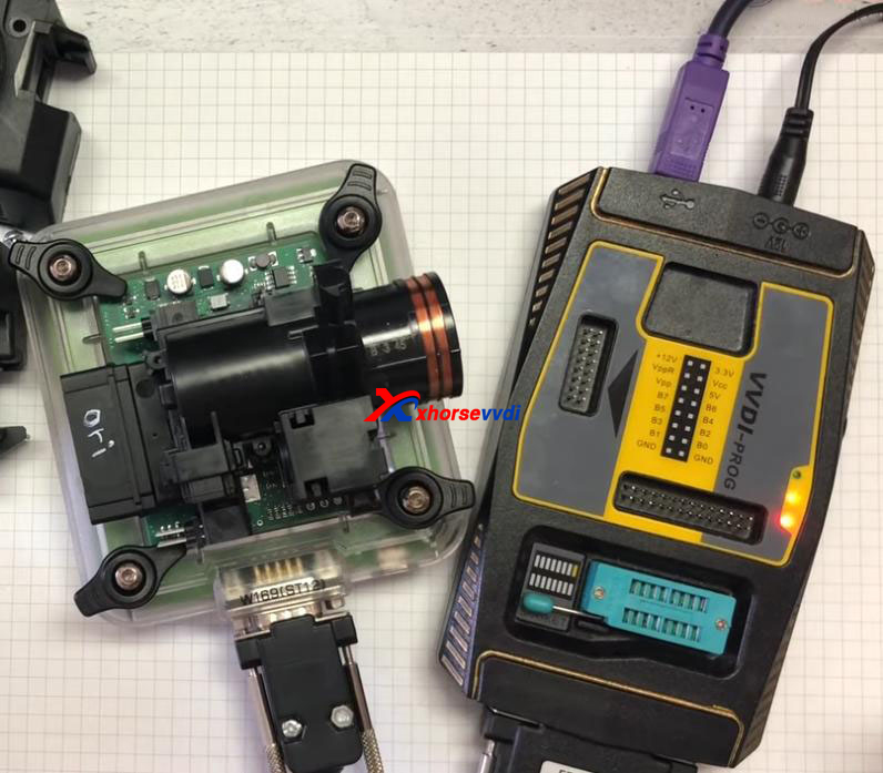
Read/Write Benz EIS/EZS W164 (ST12), W169(ST12), W203(HC08), W209/211(ZWG), W209/211(HC12), W211(ST12), W215/220/230, W639(HC08), SPRINTER(ST12), VITO W639(ST12) without soldering |
 |
Contact US:
If you have any questions, please do not hesitate to contact us.

Shipping Method and Delivery Time:
EU, US, UK ,RU Warehouse: 3-7 working days. We have stocked up hot sale items in US, UK ,RU, EU Warehouse, Fast Delivery No Tax. But if overseas warehouse is sold out, we will send from Hongkong by DHL.
EU warehouse only for EU customers. UK warehouse for UK address only! US the same, and not includes overseas territories. No customs tax.
DHL: 3-7 working days. And EU address by DHL invoice value can't be less than 150USD. If your address is remote area for DHL, need to pay remote cost about 35USD or no extra fee ship by YANWEN.
Yanwen Express: 5-17 working days. No customs Tax or remote cost for EU Countries.
About VAT, if company buyer needs the VAT invoice, please pay the VAT, then we provide VAT invoic for you to do tax refund.
Tech Support
VVDI Prog can support to read MC9S12XE, and here we will share some info about MC9S12XE Chip.
1.Dflash and EEPROM
DFLASH and EEE share a data space, which can be understood as the data space in HDD, and then DFLASH and EEE are partitions on the hard disk. For example, DFLASH is the C drive and EEE is the D drive. We can give the entire hard drive to the C drive or all to the D drive, or the C drive and D drive can exist at the same time.
The size of all MC9S12XE series chips is 32KB, if all parts are given to DFLASH, DFLASH is 32KB (BMW CAS4+ is divided in this way, so CAS4+ does not have EEE). If the entire part is given to EEE, the size of EEE is 4KB (roughly understood as 8KB of data that EEE needs to occupy per 1KB, if EEE is 4KB, all 32K of space will be fully used, such as BMW E chassis FRM) Part to DFLASH and part to EEE (DFLASH+EEE*8<=32kb, such as Land Rover KVM) EEE allocates 1K to occupy 8K of space, because part of the space is used for caching. The size of DFLASH and EEE can read the size information (that is, the partition information) under the normal condition of the chip. When using xhorse products like VVDI Prog to read the 9S12XE chip, it will automatically read the data of the corresponding size according to the chip partition information.
The following situations require attention:
.1 The chip supports direct use without partitions (similar to HDD only C drive). In this case, the partition information read is FFFFF (the software will prompt the partition is abnormal), and the actual data is DFLASH 32K, EEE no data (some modules will be like this)
*If a module prompts a partition error when reading data, but the module itself can work normally, it is used directly without partitions.
.2 There is a certain probability that the chip will lose the partition information during normal operation. In this case, the partition information read is also FFFF (for example, BMW E chassis FRM).
*In this case, the module usually does not work normally
*When the partition information is lost, it is meaningless to read the EEE space. The data read will change every time, not related to the real data.
*In the case of loss of partition information, forcibly set the size of DFLASH to 32kb, the actual DFLASH and EEE data can be read out (note that the EEE data is not real data after being read, and it needs to be converted by algorithm to become real EEE data)
.3 The chip cannot directly read EEE data through the backup read option in the encrypted state, so if you need to read EEE data like Land Rover KVM, you must unlock the chip first, and then read the EEE data.
2.Partition size and mask.
MC9S12XE series chip modules are partitioned normally;BMW CAS4+ 32KB DFALSH encrypted byte FF
The BMW CAS4 uses the VVDI reading data and do key matching, no need encryption and decryption, but it needs to be unlocked and locked in the operation of adjusting km or writing data. After unlocking, the CAS computer cannot work normally without locking it.
Land Rover KVM 4KB DFLASH 2KB EEE encrypted byte FC
Land Rover KVM computer must be unlocked when the key is matched to read the data. After the key is generated, it must be locked. If it is to write a new data OBD match, there is no need to lock
Porsche BCM The first type 32KB DFLASH The second type 16K DFLASH 2KB EEE (*No valid data in EEE) Encrypted bytes 7D
If the Porsche matching key is OBD learning, you only need to backup and read the data without decryption.
If it is a direct write start, it needs to be unlocked, and after the data is reversed written back, then the lock is performed, otherwise the vehicle cannot work normally.
The following is the mask comparison table of MC9S12XE series. When encountering the memory of unknown module, you can check the following mask to find its corresponding type in the programmer.
[MC9S12XEP100/XEP768] The left side of the following data is the mask and the right side is the chip ID
0M22E 0xCC80 1M22E 0xCC80 2M22E 0xCC82 0M48H 0xCC90 1M48H 0xCC91 2M48H 0xCC92 3M48H 0xCC93 5M48H 0xCC94 0N35H 0xCC95 1N35H 0xCC95
[MC9S12XEQ512/XET512] The left side of the following data is the mask and the right side is the chip ID 0M25J 0xC480 1M25J 0xC481 2M25J 0xC482 3M25J 0xC482 0M12S 0xC483 1M12S 0xC483 ;[MC9S12XET256] 0M53J 0xC080 1M53J 0xC081 2M53J 0xC081 0N36H 0xC082 1N36H 0xC082 ;[MC9S12XEG256] 0M53J 0xC080 1M53J 0xC081 2M53J 0xC081 0N36H 0xC082 1N36H 0xC082 [MC9S12XEA256] The left side of the following data is the mask and the right side is the chip ID 1M53J 0xC081 2M53J 0xC081 0N36H 0xC082 1N36H 0xC082
